- Industrial Design[3]
- Other Electrical Equipment[10]
- Inductors[1]
- Other Power Supplies[1]
- Switching Power Supply[3]
- Transformers[1]
- LED Displays[1]
- Double-Sided PCB[3]
- Multilayer PCB[2]
- Other PCB & PCBA[10]
- Rigid PCB[8]
- Other Lights & Lighting Products[1]
- Motor Driver[10]
- Other Motor Accessories[1]
- Pressure Gauges[1]
- Temperature Instruments[2]
- Contact Person : Ms. li sally
- Company Name : Hangzhou Singo Tech Co., Ltd.
- Tel : 86-571-87203964
- Fax : 86-571-87203614
- Address : Zhejiang,Hangzhou,6F of B Building, No.8, West Garden 1st Roard , West Lake Technopark, Hangzhou, China
- Country/Region : China
- Zip : 310012
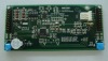
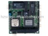
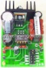
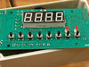
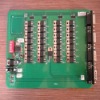
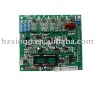
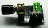
light dimmer pcba


Related Product Searches:light dimmer pcba,High Quality,light dimmer pcba, light dimmer pcba
light dimmer pcba
PCBA specific instruction
Material:FR-4
Layer: 2 layers
Surface finish, HASL lead free
Solder mask: Green
Silk screen: White
The othere surface finish we could do are; Gold finger, OSP, ENIG, HAL, Gold plating, Chemical silver, etc.
The other solder mask type we could do are: Red, yellow, white, black, purple
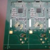
PCBA&SMT PCB&PCB SMT&electronic assembly&pcb electronic
1. PCB layout, PCB design; 2: Make high difficulty PCB(1 to 38 layers) 3: Provide all Electronic components; 4: PCB assembly; 5: Write programs for clients; 6: PCBA/finished product Test. etc…1.Specification for PCB Manufacture:
Item | Specification |
Numbr of Layer | 1-38Layers |
Material | FR-4,FR2.Taconic,Rogers, CEM-1 CEM-3,ceramic , crockery |
Metal-backed Laminate | |
Remarks | High Tg CCL Is Availabe(Tg>=170ºC) |
Finish Board Thickness | 0.2mm-6.00 mm(8mil-126mil) |
Minimun Core Thickness | 0.075mm(3mil) |
Copper Thickness | 1/2 oz min;12 oz max |
Min.Trace Width & Line Spacing | 0.075mm/0.1mm(3mil/4mil) |
Min.Hole Diameter for CNC Driling | 0.1mm(4mil) |
Min.Hole Diameter for punching | 0.9mm(35mil) |
Biggest panel size | 610mm*508mm |
Hole Positon | +/-0.075mm(3mil) CNC Driling |
Conductor Width(W) | +/-0.05mm(2mil)or |
+/-20% of original artwork | |
Hole Diameter(H) | PTH L:+/-0.075mm(3mil) |
Non-PTH L:+/-0.05mm(2mil) | |
Outline Tolerance | +/-0.125mm(5mil) CNC Routing |
+/-0.15mm(6mil) by Punching | |
Warp & Twist | 0.70% |
Insulation Resistance | 10Kohm-20Mohm |
Conductivity | <50ohm |
Test Voltage | 10-300V |
Panel Size | 110×100mm(min) |
660×600mm(max) | |
Layer-layer misregistration | 4 layers:0.15mm(6mil)max |
6 layers:0.25mm(10mil)max | |
Min.spacing between hole edge to circuity pqttern of an inner layer | 0.25mm(10mil) |
Min.spacing between board oulineto circuitry pattern of an inner layer | 0.25mm(10mil) |
Board thickness tolerance | 4 layers:+/-0.13mm(5mil) |
6 layers:+/-0.15mm(6mil) | |
Impedance Control | +/-10% |
Different Impendance |
Processing:
uses the SMT non-lead craft, meets the international environmental protection requirement.
Optional housing materials: Aluminum alloy, ABS, or other materials.Lead time of prototype: 1. 10-15days, with customers complet
ed technical information.2. 12-18days, with customers samples 3. 20-25days, with customers request and our new design
light dimmer pcba